A7125--2.4GHz 2M datarate FSK Transceiver
1. Typical Application
2.4GHz ISM band Communication System ? Wireless Intelligent sports
2.4GHz Remote Control ? Wireless Toy and Gaming
Wireless Keyboard and Mouse ? Wireless Audio/Video Streaming
2. General Description
A7125 is a high performance and low cost 2.4GHz ISM band wireless transceiver. It integrates high sensitivity receiver(-90dBm @2Mbps), high efficiency power amplifier (up to 3dBm), frequency synthesizer and base-band modem. In typical system, A7125 is used together with MCU (microcontroller) with very few external passive components. A7125 supports both FIFO mode and direct mode that contains clock recovery circuit CKO pin to MCU.
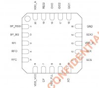
A7125 supports very fast settling time (90 us) for frequency hopping system. For packet handling, A7125 has built-in separated 64-bytes TX/RX FIFO (could be extended to 256 bytes) for data buffering and burst transmission, CRC for error detection, FEC for 1-bit data correction per code word, RSSI for clear channel assessment, data whitening for data encryption/decryption, thermal sensor for monitoring relative temperature. Those functions are very easy to use while developing a wireless system. All features are integrated in a small QFN 4X4 20 pins package.
A7125’s data rate is up to 2Mbps and can be easily programmed to 1Mbps or 2 Mbps via 3-wire or 4-wire SPI bus. For power saving, A7125 supports sleep mode, idle mode, standby mode. For easy-to-use, A7125 has an unique SPI command set called Strobe command that are used to control A7125’s state machine. Based on Strobe commands, from power saving, TX delivery, RX receiving, channel monitoring, frequency hopping to auto calibrations, MCU only needs to define A7125’s control registers and send Strobe commands via SPI bus. In addition, A7125 supports two general purpose
I/O pins, GIO1 and GIO2, to inform MCU its status so that MCU could use either polling or interrupt scheme to do radio control. Therefore, it is very easy to monitor transmission between MCU and A7125 because of its digital interface.
3. Feature
Small size (QFN 4X4, 20 pins).
Support 2400 ~ 2483.5 MHz ISM band.
FSK modulation.
Programmable data rate to 1Mbps or 2Mbps.
Low current consumption: RX 17mA, TX 15.7mA (at 0dBm output power).
Low sleep current (1.5uA).
Programmable RF output power -20dBm ~ 3dBm.
Very High sensitivity (-90dBm@2Mbps, -92dBm@1Mbps).
On chip regulator, supports input voltage 2.0 ~ 3.6V.
Easy to use
Support 3-wire or 4-wire SPI.
Unique Strobe command via SPI.
Change frequency channel by ONE register setting.
8-bits Digital RSSI for clear channel indication.
Fast exchange mode during TRX role switching.
Auto RSSI measurement.
Auto Calibrations.
Auto IF function.
Auto CRC Check.
Auto FEC by (7, 4) Hamming code (1 bit error correction / code word).
Data Whitening for encryption and decryption.
Separated 64 bytes RX and TX FIFO.
Easy FIFO / Segment FIFO / FIFO Extension (up to 256 bytes).
Support direct mode with recovery clock output to MCU.
Support direct mode with frame sync signal to MCU.
Support low cost crystal (6 / 8 /12 / 16MHz).
Support low accuracy crystal within ± 50ppm.
Support Auto Frequency Compensation.
Support crystal sharing, (1 / 2 / 4 / 8MHz) to MCU.
Fast settling time synthesizer for frequency hopping system.
Built-in thermal sensor for monitoring relative temperature
Built-in Battery Detector.

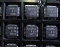 M30260F8AGP Renesas
  全新原装正品STM32F103C8T6
  LM2596ADJ TO-263 波形稳
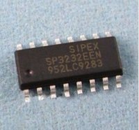 SP3232EEN SOP16 马来西亚
 产品名称:【供应】A7125--2.4G无线音频RF IC